Technical data Characteristic curve of a Zener diodeArticle no: P1377900 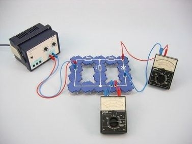
<!DOCTYPE html PUBLIC "-//W3C//DTD XHTML 1.0 Transitional//EN"
"http://www.w3.org/TR/xhtml1/DTD/xhtml1-transitional.dtd">
Principle Zener diodes are silicone diodes with a high level of p and
n area doping. They behave like normal Si-diodes in the forward
direction. Voltage connected in the reverse direction produces a
strong electric field in the barrier layer. When the voltage
dependent on the preselected doping level, the breakdown voltage,
is exceeded, the electric field causes pairs of charge carriers to
be released, resulting in a sharp increase in current. This causes
the diode resistance to decrease. If the external voltage is
increased even further, then the diode current increases sharply.
This results in an increase in voltage at the multiplier while
the increase in voltage at the diode is minimal. It is important to
have the right sized multiplier to ensure that the product of
the breakdown voltage and diode current (dissipation power) does
not exceed the nominal value for the diode type. Exceeding the
nominal value alters the barrier layer, rendering it useless and
effectively destroying it. Benefits
Tasks How do Zener diodes differ from normal rectifier diodes? Investigate the relationship between current and voltage for a Zener diode in forward and reverse direction.
Scope of delivery
| |||||||||||||||||||||||||||||||||||||||||||||||||||
Robert-Bosch-Breite 10 – 37079 Göttingen – Germany
www.phywe.com